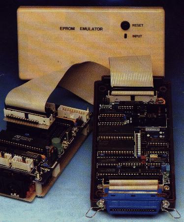
The EPROM Emulator, presented here by Keith Rickard, can be used with the Z88 to make developing ROM-based applications easier.
The Eprom emulator is a device which is connected to the parallel port of your PC (or Amiga) and allows you to send a Z88 Eprom image from a file to the emulator, using the DOS command: COPY filename LPT1:/B
The other end of the emulator is connected to a special card which is plugged into a slot in the Z88. The upshot is that the Z88 thinks it has a bona fide Eprom card in its slot and reacts to the image in the normal way. It could be an application or simply a file Eprom.
It can emulate 8K (not that useful!), 16K, 32K and 64K Eprom cards. It takes about 5 seconds for the image to be download from the PC. Obvious uses for this device (as deployed by myself) are improved ease for developing Z88 applications, downloading files to the Z88 and looking at other peoples application ROM images (have had Manic Miner and Camelot working through it!).
Building the EPROM emulator
From pages 14 to 20 of the ELEKTOR ELECTORNICS SEPTEMBER 1992 magazine.
EPROM EMULATOR II
This is a revamped version of an EPROM emulator we published about three years
ago. This time we propose to build the circuit with standard size components
rather than SMA (surface mount assembly) components, which some of you have
found difficult to obtain as well as handle. The present version of the
emulator has a RAM of 64 KByte, and is capable of emulating 2764s up to and
including 27512s. Also, by parallel connection of Centronics cables,
extensions to bus widths of 16 bits or 32 bits are easier than before.
MAIN SPECIFICATIONS
� Emulates EPROMs 2764 through 27512
� Connected to Centronics port
� Auto reset function
� 8-, 16- or 32-bit configuration
� No driver software required; use is made of existing system
utilities (MS-DOS, Windows, ST and Amiga)
Design by B.C. Zschocke and N. Breidohr
AN EPROM emulator replaces the EPROM in a computer system (to which a program
is to be developed) by RAM that behaves like an EPROM. The advantages are
well-known: the contents of the RAM can be overwritten as many times as you
like, and the data transfer from the PC (running an assembler) to the target
system is much faster. Errors in the object program are thus easily and
quickly corrected, because it is no longer necessary to remove the EPROM,
erase it, and reprogram it.
The data transfer from the PC to the emulator described here does not require
special file formats like Intel-Hex, Tektronics or Motorola. Instead,
standard system utilities can be used to output the previously prepared binary
file via the Centronics port.
Application range
The present emulator replaces the byte-organized EPROMs with a capacity of
8 KBytes (2764) to 64 KBytes (27512). The now obsolete 2-KByte and 4-KByte
EPROMs Types 2716 and 2732 may also be emulated with the aid of a specially
prepared adaptor board. Up to four emulators may be connected in parallel
to 'attack' systems with a bus width of 32 bits. The EPROM data may be
furnished by any computer system with a Centronics port. The STROBE pulses
supplied by the computer have four functions.
(1) they indicate that the data is stable and valid;
(2) they enable the emulator;
(3) they clock three-state counters IC7, IC8 and 1C9; and
(4) they select a particular emulator in 16-bit or 32-bit systems.
The counter outputs address two RAM ICs with a capacity of 32 Kbyte each. The
data applied to the input of the emulator is 'acknowledged', and copied
directly into the RAM. The selection of the RAMs is accomplished via A15 of
counter IC9, and one half of IC12. After the last byte has been stored in
the RAM, the counter is switched to high-impedance output mode
('three-state'). The individual RAM addresses are then available for selection
through the address buffer, and can be read via the data output buffer. The
addressing of the RAM at this stage is accomplished by the host system, i.e.,
the computer system or (more generally) application circuit whose EPROM is
emulated.
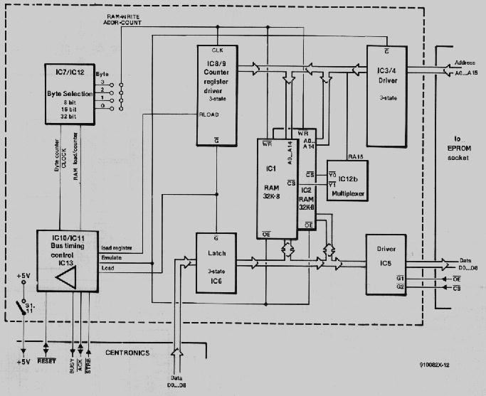
Circuit description
Essentially, the circuit consists of three blocks:
(1) A control section around IC10 and IC11, which serves to ensure the
proper bus timing on the Centronics interface, and generate a number of
internal signals. This section also supplies the RESET signal for the
application circuit (Auto-RESET). All signals are taken to the 'outside
world' via open-collector buffers/drivers contained in IC13. One driver
serves to generate the strobe signal.
(2) A byte selection circuit (IC7 and one half of IC12), which arranges the
distribution of the received 8-bit data between parallel emulators in 16-bit
and 32-bit applications. This circuit is required only if a 16-bit or 32-bit
extension is envisaged.
(3) A RAM address and load address generator consisting of a counter (IC8 and
IC9) that supplies the RAM addresses during loading, a latch (IC6) for
intermediate storage of Centronics databytes, and drivers (IC3, IC4 and IC5)
that interface to the EPROM socket in the application circuit. Depending on
the mode of operation of the circuit (loading or emulating), either the
counter/latch combination or the EPROM socket interface are in control of the
EPROM addresses and data.
Since 64-Kx8-bit RAMs are not easily obtained at reasonable prices, the
present emulator is based on two 32-Kx8-bit RAMS. These offer a total storage
capacity of 64 KByte, and allow the emulator to mimic EPROMs up to and
including the 27512. When smaller EPROMs are used, address lines A15
(27256), A15/A14 (27128) or A15/A14/A13 (2764) must be tied to ground via
the appropriate jumpers (see Table 1).
Operation in detail
The Centronics standard stipulates that data must be stable for a certain
time before and after the STROBE pulse. This ensures freedom of using either
the leading or the trailing edge of the strobe signal to capture data from
the printer's Centronics input. In the emulator, both edges are used.
At power-up, R7 and C7 provide a defined state. Bistables IC11a and IC11b
are set, while bistables IC10a and IC10b are reset. IC1lb clears all
counters, and switches the circuit to the emulate mode. With reference to
the timing diagram of the 8-bit version (Fig. 2), the negative edge of the
STROBE signal triggers IC10b, and resets IC1la and IC11b. Next, IC11b
switches the circuit to load mode, and actuates the RESET line. IC11a
actuates the Centronics BUSY line, and the positive edge at its output causes
the counter state to be transferred to the counter register, and the
Centronics databyte to be transferred to the latch. Data and address are
allowed to stabilize at the respective RAM inputs while the STROBE pulse
lasts. The positive edge of the STROBE pulse triggers IC10a, and actuates
the RAM WRITE signal and the Centronics ACKNLG (acknowledge) signal during
the monotime of IC10a. The signal edge that marks the monotime sets IC11a,
and so clears the BUSY signal. At the same time, the counter is advanced one
state. The first byte has been stored in RAM, and the circuit is ready to
receive the next byte. A byte received within the monotime of IC10b causes
this monostable to be triggered again. Otherwise, the above cycle starts
again on detection of the negative edge of the STROBE pulse. If no databyte
is received during the monotime of 1C10b, the circuit switches to emulate
mode, clears the RESET signal, switches the counters to three-state, and
resets them. At this point, the RAM addressing is taken over by the
application circuit.
To prepare the circuit for use in 16-bit or 32-bit applications, 1C7 and one
half of IC12 divide the internal RAM WRITE and counter output signals.
Depending on the jumper setting, either the each first, second, third or
fourth byte is copied into the latch, while the counters receive an
appropriately reduced number of clock pulses. The RAMs are switched via
their CS (chip select) lines, with the aid of address line A15 and the other
half of IC12.
At first glance, the outputs Of IC10b and IC11b behave identically. Why,
then, are both used? The timing diagram shows an unexpected, rather
unwelcome, quirk of the monostable, IC10b. At the (relatively long)
monotime, the time between the triggering instant and the output actuation
instant is not short enough. This caused problems in a number of prototypes.
The trigger signal supplied by IC10b actuates IC11b instantly, while IC11b
is de-actuated again by the negative edge Of IC10b. Capacitor C6 may also
cause trouble if it cannot be discharged quickly enough by IC10. Increasing
its value must, therefore, be done with care.
LED D1 lights when the computer feeds data into the emulator. The
(active low) RESET signal is taken to the application circuit via connector
K2. On completion of the load activity, the emulator releases the RESET line,
and so re-starts the application circuit, which subsequently runs its new
software contained in the emulator RAM.
The emulator is powered either by the application circuit (via Sl-10), or by
the onboard stabilizer (via S1-9), whose input is connected to a small mains
adaptor with d.c. output. Whether or not an external power supply is
required is, of course, dependent on the capacity of the target system's
power supply. A power supply conflict may arise when the emulator is powered
by the application circuit, and this is switched off, or powered down during
reset, while the 'other side' of the emulator is connected to the PC (which
is still on) via a Centronics cable. If this happens, the emulator is powered
via the protection diodes in the Centronics interface of the PC. This results
in a supply voltage of about 3V, which is sufficient for the RAMs to retain
their data, but not for the TTL circuits to operate properly. If, in this
condition, the application circuit is switched on, the emulator may go into
an undefined state, which may be ended by pressing a button connected between
point 'S' and ground. A better solution, however, is to power the emulator
from an external source via IC14. The previously described power supply
conflict may also damage the emulator, because the current sent into the
application circuit via the EPROM socket may become so high that the driver
Ics are destroyed.
Practical hardware
The printed circuit board designed for the EPROM emulator is a high-density
double-sided, through-plated type, which is best purchased ready-made through
our Readers' Services. Space is pretty tight on the board, so keep an eye on
the pitch of the capacitors. Capacitor C11 is fitted at the solder side of
the board, underneath IC1.
Pin header K1 is suitable for two types of connection: its pinning is
compatible with a 25-way sub-D connector (allowing ready use of IDC-style
connectors), as well as with a 36-way Centronics socket. When the latter
is used, make sure to remove pins 4 and 6, or cut the relevant tracks.
When a 25-way sub-D connector is used, it is, unfortunately, not possible to
create a 'loop-through' connection for the supply voltage. To reduce cost,
a 40-way IDC socket was used on the prototype - a 26-way type (for connection
to sub-D plug) is, of course, also possible.
The 16-bit and 32-bit versions of the EPROM emulator require two or four
col plete circuits, respectively, which are driven by a common line, for
instance, via four IDC-style Centronics plugs. The jumper settings on each
board may be found in Table I The emulators are mutually synchronized via the
ACK line on the Centronics interface The BUSY line may be connected on one
board only (S1-12). In case the emulators are to be powered by a single,
external, supply this is connected to one board only, from where the supply
voltage is distributed via pin S1-11 on each board. On the board from which
the supply voltage is distributed, S19 must be closed. On all other boards,
Sl-9 is open. Sl-10 must be closed on all boards.
Software
As already mentioned, special software is not strictly required. The emulator
RAM can be loaded with the aid of any system capable of outputting binary
files in form, via the Centronics port. This that the EPROM emulator can be
used with any computer sporting a Centronics-com ipatible printer port.
Users of MS-DOS PCs may want to obtain version 2.0 of EPROMSIM, a program
which is available on disk through our Readers Services as item ESS129.
EPROMSIM supports EPROMs up to 64 KByte, and is capa ble of handling the
following 'intelligent file formats:
� Intel Intellec-8;
� Tektronix hexadecimal;
� Motorola.
Construction
When building the circuit, remember to remove pins 4 and 6 of the Centronics
socket if used. To ensure ready access, the DIP switch array is best mounted
on IC sockets. Alternatively, you may want to fit the switches at the solder
side of the board, and cut a clearance in the back panel of the enclosure.
The LED wires may be extended to enable the LED to be fitted in a hole in the
cover panel. Further constructional points that deserve your attention are
the mounting of the Centronics input socket, and the strain relief on the
flatcable to the EPROM adaptor.
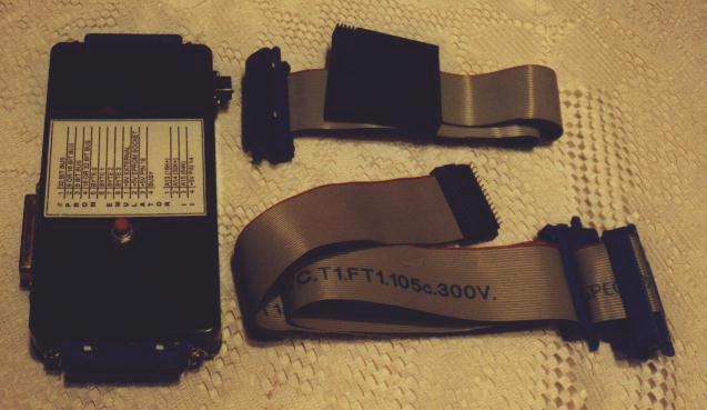
The EPROM adaptor is home-made. As shown in Fig. 5, it consists of a piece
of strip board, two lengths of IC pin strip, a box header and two 28-way
IC sockets. The flatcable from the EPROM emulator is fitted with a 28-way
IDC socket. You may want to make one adaptor for each EPROM type, and wire
jumpers A13, A14 and A15 appropriately, direct on the socket. Wires 29 to
34 of the flatcable are connected to the RESET generator on the emulator
board, and may also be taken to the adaptor socket to create a RESET
connection for the application circuit.
DOWNLOADING TO THE EPROM EMULATOR
PC/MS-DOS COPY LPT1:/B (/B for binary output)
Amiga COPY PAR: (PAR:, not PRT:)
TOS On the ST it is sufficient to double-click on the filename shown on
the desktop, and then output to 'printer'. It should be noted,
however, that the TOS appends a CR/LF sequence to each file.
This means that the last two bytes of a 32-Kbyte file can not be
used. However a simple printer manager that does not output the
CR/LF sequence should not be too difficult to write in Pascal, C
or BASIC.
COMPONENTS LIST
Resistors:
6 10k Ohm R1;R2;R4;R5;R8;R12
1 470 Ohm R3
1 1M Ohm R6
4 100k Ohm R7;R9;R10;R11
2 7-way 10k Ohm SIL R13;R14
Capacitors:
Pitch 0.2 inch (5mm)
1 470uF 16V radial C1
2 330nF C2;C7
11 100nF C3;C8-C18
1 1nF C5
Pitch 0.1 inch (2.5)
1 100uF 16V radial C4
1 2uF2 16V radial C6
Semiconductors:
1 LED, green, 3mm D1
2 62256 (<100ns) IC1;IC2
3 74HCT541 IC3;IC4;IC5
1 74HCT574 IC6
3 74HC590 IC7;IU8;IC9
1 74HCT123 IC10
1 74HCT74 IC11
1 74HCT139 IC12
1 7407 (or 74LS07) IC13
1 7805 IC14
Miscellaneous:
1 12-DIP switch block, or 24-way pin header block with jumpers
S1
1 40-way box header K1
1 34-way box header K2
1 40-way IDC socket
1 34-way IDC socket
1 IDC Centronics socket
1 TO-220 style heatsink
1 Printed circuit board 910082
1 ABS enclosure; approx. size 160x80x32mm
IC sockets
28-way DIL adaptor (see Fig.5)
Approx 50cm 36-way flatcable
Per the September 1992 magazine, the circuit board 910082 can be purchased
for �8.50 + VAT (�9.99) from:
ELEKTOR ELECTRONICS (PUBLISHING)
P.O. BOX 1414
Dorchester
DT2 8YH
England
Method of payments available:
� Bank draft
� Cheque (made payable to Elektor Electronics)
� Giro transfer (account no. 34 152 3801)
� Postal order
� Visa, Acces, Mastercard, Eurocard.